- SixCarbon News
2018-12-07 Our paper is published on AFM:Controlled Doping of Wafer‐Scale PtSe2 Films for Device Application

Abstract
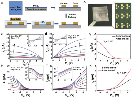
Semiconductive transition metal dichalcogenides (TMDs) have been considered as next generation semiconductors, but to date most device investigations are still based on microscale exfoliation with a low yield. Wafer scale growth of TMDs has been reported but effective doping approaches remain challenging due to their atomically thick nature. This work reports the synthesis of wafer‐scale continuous few‐layer PtSe2 films with effective doping in a controllable manner. Chemical component analyses confirm that both n‐doping and p‐doping can be effectively modulated through a controlled selenization process. The electrical properties of PtSe2 films have been systematically studied by fabricating top‐gated field effect transistors (FETs). The device current on/off ratio is optimized in two‐layer PtSe2 FETs, and four‐terminal configuration displays a reasonably high effective field effect mobility (14 and 15 cm2 V?1 s?1 for p‐type and n‐type FETs, respectively) with a nearly symmetric p‐type and n‐type performance. Temperature dependent measurement reveals that the variable range hopping is dominant at low temperatures. To further establish feasible application based on controllable doping of PtSe2, a logic inverter and vertically stacked p–n junction arrays are demonstrated. These results validate that PtSe2 is a promising candidate among the family of TMDs for future functional electronic applications.

